
The demand for Single Crystal Quartz Wafers continues to rise as industries such as telecommunications, semiconductor manufacturing, aerospace, precision sensing, and medical electronics require increasingly reliable piezoelectric materials. These wafers are essential for producing high-performance frequency control devices, resonators, oscillators, and SAW (Surface Acoustic Wave) components, where even microscopic defects can impact device performance.
Manufacturing Single Crystal Quartz Wafers is a highly specialized process that combines crystal growth, precision machining, chemical processing, and rigorous quality control. Every production stage presents unique challenges that manufacturers must overcome to achieve exceptional crystal quality, dimensional accuracy, and electrical performance. CQT has extensive expertise in producing high-quality quartz wafers that meet the stringent requirements of advanced electronic applications.
Unlike conventional glass or polycrystalline materials, single crystal quartz has a highly ordered atomic structure. Preserving this crystal integrity throughout the manufacturing process is critical because defects can affect frequency stability, piezoelectric performance, and long-term reliability.
Key manufacturing objectives include:
· Maintaining crystal purity
· Preventing lattice damage
· Achieving precise crystallographic orientation
· Producing ultra-flat surfaces
· Minimizing contamination
· Ensuring consistent wafer thickness
Meeting all these requirements simultaneously demands advanced equipment, skilled engineering, and strict process control.
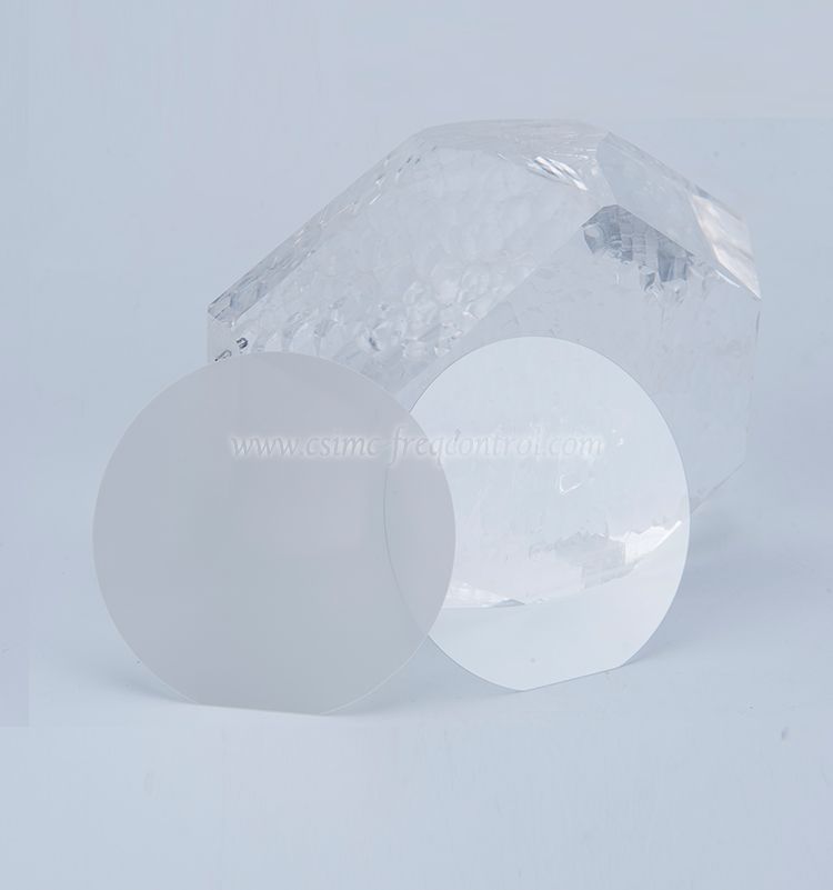
The manufacturing process begins with growing synthetic quartz crystals under carefully controlled hydrothermal conditions.
Maintaining crystal purity is essential because impurities may lead to:
· Electrical instability
· Reduced frequency accuracy
· Lower piezoelectric efficiency
· Increased defect density
Manufacturers carefully control temperature, pressure, nutrient composition, and growth duration to produce large, high-quality crystals suitable for wafer fabrication.
Even during crystal growth, defects can develop, including:
· Inclusions
· Dislocations
· Twinning
· Internal stress
· Growth striations
These imperfections may reduce wafer yield and negatively impact downstream device performance.
Advanced monitoring and optimized growth parameters help minimize defect formation.
One of the defining characteristics of Single Crystal Quartz Wafers is their precise crystallographic orientation.
Depending on the intended application, manufacturers produce wafers using various crystal cuts, including:
· AT-cut
· BT-cut
· SC-cut
· X-cut
· Y-cut
· Z-cut
Even a slight deviation from the specified orientation can alter:
· Resonant frequency
· Temperature stability
· Frequency drift
· Device sensitivity
Precision orientation equipment is therefore essential during wafer preparation.
Quartz is both hard and brittle, making precision cutting particularly challenging.
During slicing, manufacturers must prevent:
· Edge chipping
· Surface cracking
· Microfractures
· Excessive material loss
High-precision diamond wire saws and optimized cutting parameters help minimize mechanical stress.
Every cutting operation removes a small amount of material known as kerf.
Reducing kerf loss improves:
· Material utilization
· Manufacturing efficiency
· Production yield
· Overall cost-effectiveness
Modern cutting technologies continue to improve material recovery while maintaining dimensional accuracy.
After slicing, wafers undergo grinding and lapping to achieve uniform thickness.
This stage presents several challenges.
Many electronic applications require thickness tolerances measured in micrometers.
Uneven thickness may cause:
· Frequency variation
· Mechanical stress
· Reduced device consistency
· Lower production yield
Manufacturers use automated measurement systems throughout the process to ensure excellent thickness control.
Grinding introduces microscopic surface damage that must be removed during subsequent polishing.
Improper process control may leave:
· Scratches
· Residual stress
· Surface fractures
· Subsurface defects
Carefully controlled abrasive selection helps minimize these issues.
Polishing is one of the most critical manufacturing stages for Single Crystal Quartz Wafers.
High-quality wafers require mirror-like surfaces with extremely low roughness values.
Poor polishing can introduce:
· Surface waviness
· Fine scratches
· Local defects
· Reduced bonding quality
Chemical mechanical polishing (CMP) is commonly used to produce exceptionally smooth surfaces suitable for demanding electronic applications.
Besides surface smoothness, wafer flatness directly affects downstream processing.
Manufacturers closely monitor parameters such as:
· Total Thickness Variation (TTV)
· Bow
· Warp
· Surface flatness
High flatness improves photolithography alignment and device fabrication accuracy.
Tiny particles can significantly reduce wafer quality.
Potential contamination sources include:
· Abrasive residues
· Dust
· Tool wear particles
· Human handling
Manufacturing is therefore performed inside cleanroom environments with strict contamination control procedures.
Cleaning chemicals must effectively remove contaminants without damaging the quartz surface.
Multiple cleaning and rinsing stages ensure wafers meet stringent cleanliness standards before packaging.
Every production stage includes detailed inspections to verify product quality.
Common inspection methods include:
Automated optical systems detect:
· Surface scratches
· Chips
· Cracks
· Contamination
High-precision instruments confirm uniform wafer thickness across the entire surface.
X-ray diffraction and other advanced measurement systems verify crystal orientation with exceptional accuracy.
Surface roughness, flatness, and defect density are evaluated to ensure compliance with customer specifications.
Yield optimization remains one of the greatest manufacturing challenges.
Manufacturers continuously improve:
· Crystal growth consistency
· Equipment precision
· Process automation
· Statistical process control
· Operator training
These improvements reduce scrap while maintaining consistent product quality.
CQT specializes in manufacturing premium Single Crystal Quartz Wafers for demanding electronic, semiconductor, and communication applications. By combining advanced crystal growth technology with precision machining and comprehensive quality control, CQT delivers products that meet the highest industry standards.
Key advantages include:
· High-purity synthetic quartz crystals
· Precise crystallographic orientation
· Excellent thickness uniformity
· Ultra-flat polished surfaces
· Low defect density
· Strict cleanroom manufacturing
· Comprehensive quality inspection
· Customized wafer specifications for various applications
These capabilities enable CQT to supply reliable quartz wafers for frequency control devices, sensors, RF components, and advanced semiconductor technologies.
High-quality Single Crystal Quartz Wafers are widely used in:
· Quartz crystal resonators
· Oscillators
· Surface Acoustic Wave (SAW) devices
· Frequency filters
· Precision timing modules
· MEMS sensors
· Aerospace electronics
· Medical equipment
· Industrial automation systems
· Advanced communication technologies
As demand for higher-frequency and more reliable electronic devices continues to grow, the importance of precision-manufactured quartz wafers will only increase.
Manufacturing Single Crystal Quartz Wafers involves a series of highly controlled processes, each presenting unique technical challenges. From crystal growth and orientation control to precision cutting, polishing, contamination management, and quality inspection, every stage influences the final wafer's performance and reliability.
Manufacturers that invest in advanced equipment, rigorous process control, and comprehensive quality assurance are better positioned to deliver wafers that meet the demanding requirements of modern electronics. With its expertise in crystal growth, precision processing, and strict quality management, CQT provides high-performance Single Crystal Quartz Wafers that support the next generation of semiconductor, telecommunications, sensing, and frequency control technologies.
Previous: Why Quartz Glass Substrates Are Used in High-Temperature Optical Systems
Next: Why Lithium Tantalate Wafers Remain Important in High-Temperature SAW Devices
Copyright:@2020-2021

Comments Please sign in or sign up to post.
0
0 of 500 characters used