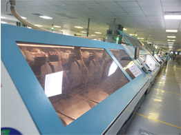
Because user applications require more and more board layers, the alignment between layers becomes very important. Inter-level alignment requires tolerance convergence. As board size changes, this convergence requirement is more demanding. All layout processes are produced in a controlled temperature and humidity environment. The exposure equipment is in the same environment, and the registration tolerance of the front and rear images of the entire area must be maintained at 0.0125mm. In order to achieve this accuracy requirement, the alignment of the front and rear layouts needs to be completed with a CCD camera.
After etched, a four-drilling system was used to perforate the inner plate. The perforation passes through the core plate, the position accuracy remains 0.025mm, and the repeatability is 0.0125mm. Then use a pin to insert the perforation to align the etched inner layer and bond the inner layers together. Initially, the use of this post-etching perforation method can fully ensure the alignment of the drilled holes and the etched copper plate, forming a rugged ring-shaped design structure. However, as users require more and more wiring in a smaller area in terms of Prototype PCB routing, in order to keep the fixed cost of the board unchanged, the size of the etched copper plate is required to be smaller, and thus the interlayer copper plate is better. Ground position. To achieve this goal, the purchase of X-ray drilling machines can be used. The device can achieve a position accuracy of 0.025mm when drilling a hole on a board with the largest specification of 1092 × 813mm.There are two ways to use it, as a PCB Prototype Service Supplier, to tell you:
1. Use an X-ray machine to observe the etched copper on each layer, and determine an optimal position by drilling.
2. The drilling machine stores statistical data and records the deviation and divergence of the alignment data from the theoretical value. This SPC data is fed back to the previous processing steps such as the selection of raw materials, processing parameters and layout drawing, etc., to help reduce its rate of change and continuously improve the process.
Although the plating process is similar to any standard plating process, there are two major differences that must be considered due to the unique characteristics of the large backplane.
Jigs and conveying equipment must be able to transfer both large and heavy boards at the same time. The 1092x813mm (43x32 inch) large format raw material substrate can weigh up to 25 kilograms (56 pounds). The substrate must be securely grasped during transportation and processing. The design of the tank must be deep enough to accommodate the board, and the entire box must maintain uniform plating characteristics.
In the past, users have specified press-fit connectors for backplanes, so they rely heavily on the uniformity of copper plating. The thickness of the back plate varies from 0.8mm to 10.0mm. The existence of various aspect ratios and the increase in the size of the substrate make the uniformity index of the electroplating very important. To achieve the required uniform performance, periodic reverse plating control equipment must be used. In addition, the necessary stirring must be performed to keep the plating conditions as uniform as possible.
In addition to the uniform thickness of the plating layer required for drilling, backplane designers generally have different requirements for the uniformity of copper on the surface of the outer layer. Some designs etch very few signal lines on the outer layer. On the other hand, in the face of the needs of high-speed data rates and impedance control circuits, it is necessary to provide a nearly solid copper foil on the outer layer for EMC shielding.
Our company also sells Flexible PCB, welcome to consult.
Copyright:@2020-2021
Comments Please sign in or sign up to post.
0
0 of 500 characters used