
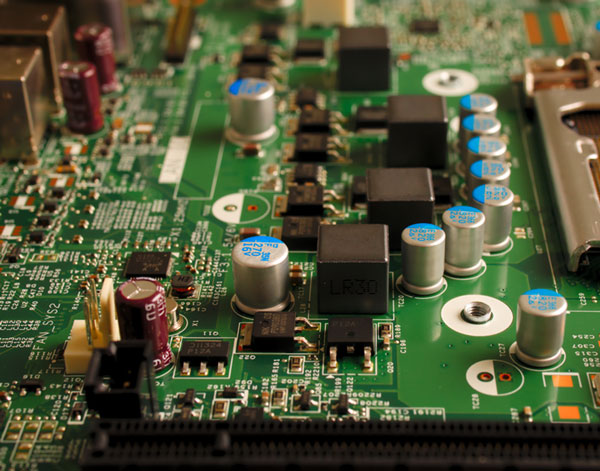
Printed Circuit Boards (PCBs) are integral to modern electronic devices, providing the necessary pathways for electrical currents to power components and enable communication between them. The manufacturing process of PCBs is intricate and involves several stages to ensure precision and reliability. This detailed guide explores each step of the PCB manufacturing process, from initial design to final inspection.
The journey of PCB manufacturing begins with the design and layout phase. This stage involves creating a detailed schematic of the circuit and a corresponding layout using CAD (Computer-Aided Design) software. The design includes the placement of components, routing of electrical connections, and defining the layers of the PCB. The finalized design is converted into a Gerber file format, which is the industry standard for PCB manufacturing.
Once the design is finalized, the next step is to prepare the materials. The base material, typically fiberglass (FR4), is coated with a layer of copper on one or both sides. This copper-clad laminate serves as the foundation for the PCB. For multilayer PCBs, multiple layers of this laminate are prepared.
In this step, the inner layers of the PCB are printed with the circuit design. A photoresist material is applied to the copper-clad laminate, and the design is transferred using UV light exposure through a photomask. The exposed photoresist hardens, while the unexposed areas remain soft and are subsequently washed away, revealing the copper pattern underneath.
After imaging, the next step is etching. The PCB is exposed to a chemical solution that removes the unprotected copper, leaving only the desired copper traces. This process creates the necessary electrical pathways on the inner layers.
For multilayer PCBs, the individual layers are laminated together. The inner layers, with their etched copper patterns, are stacked and aligned with layers of prepreg (pre-impregnated with resin) and outer copper layers. This stack is subjected to high temperature and pressure, causing the prepreg to melt and bond the layers together, forming a single cohesive board.
Once laminated, the PCB undergoes drilling to create holes for component leads and vias (holes that allow electrical connections between layers). Precision drilling machines are used to create these holes, ensuring accuracy and consistency.
After drilling, the holes need to be plated to establish electrical connectivity
between the different layers. The board is subjected to a series of chemical baths that deposit a thin layer of copper onto the walls of the holes, creating conductive pathways that connect the various layers of the PCB.
The outer layers of the PCB now undergo a similar imaging and etching process as the inner layers. A photoresist material is applied, the circuit design is transferred using UV light, and the unwanted copper is etched away. This step creates the final copper traces on the top and bottom surfaces of the PCB.
A solder mask is applied to the PCB to protect the copper traces from oxidation and to prevent solder bridges during component assembly. The solder mask is a layer of insulating material that covers the entire board except for the pads where components will be soldered. It is usually green but can come in other colors as well.
To enhance solderability and protect the exposed copper pads, a surface finish is applied. Common finishes include HASL (Hot Air Solder Leveling), ENIG (Electroless Nickel Immersion Gold), and OSP (Organic Solderability Preservatives). Each finish has its advantages and is chosen based on the specific requirements of the PCB.
The silkscreen layer is applied to the PCB to add labels, component designators, and other markings that aid in assembly and troubleshooting. This layer is typically white and printed using a screen printing process or advanced inkjet printing techniques.
Before the PCB is shipped, it undergoes rigorous electrical testing to ensure that all connections are correct and that there are no shorts or open circuits. Testing methods include:
Automated Optical Inspection (AOI): Uses cameras to inspect the PCB for defects.
Flying Probe Testing: Uses probes to test electrical continuity without the need for a custom test fixture.
In-Circuit Testing (ICT): Involves using a fixture to test each node on the PCB.
In addition to electrical testing, the PCB undergoes a final visual inspection to check for any physical defects or imperfections. This step ensures that the PCB meets all design specifications and quality standards.
After passing all inspections and tests, the PCBs are carefully packaged to prevent damage during transit. Proper packaging is crucial to protect the PCBs from environmental factors and mechanical stress.
The PCB manufacturing process is a complex and highly precise procedure that involves multiple stages, each critical to the final quality and performance of the board. From design and material preparation to imaging, etching, and testing, every step must be executed with meticulous attention to detail. By understanding
the intricate process of PCB manufacturing, companies and engineers can better appreciate the craftsmanship and technology that go into producing reliable and high-performance circuit boards. Whether for consumer electronics, automotive systems, or advanced industrial applications, PCBs are the backbone of modern electronics, and their quality directly impacts the functionality and longevity of the end products.
Copyright:@2020-2021

Comments Please sign in or sign up to post.
0
0 of 500 characters used